믿 을 만 한 PCB 회로 제조 업 체!! Contact Us

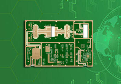

모델:F4BM PTFE PCB
D K:2.65
레이어:2Layers
Dielectrics 두께 :1.524mm(60mil)
Finished 두께 :1.6mm
Material Cu 두께 :½(17μm)HH/HH
Finished Cu 두께 :1OZ(35μm)
표면처리:Immersion Silver
응용 영역:Automotive Radar, Radio Frequency Coupler,Radar Gauges
전자 설비의 고주파화 는 발전 추세이다. 특히 무선 네트워크 와 위성통신이 날로 발전함에따라 정보 제품은 고속화, 고주파화되고 통신 제품 은 음성 표준화 방향으로 발전 하고있다.대용량, 고속무선으로 전송되는 영상 과 데이터, 위성 시스템, 휴대 전화 수신 기지국 등 통신 제품 은 반드시 고주파회로 기판을 사용해야한다.앞으로 몇년내에 그것은 신속하게 발전하여 고주파판에 대한 수요량이 매우 클것이다.
고주파판 재료의 기본 특성은 다음과 같다:
(1) The DK must be small and stable. Generally, the smaller the better, the signal transmission rate is inversely proportional to the square root of the dielectric constant of the material. High dielectric constant can easily cause signal transmission delay.
(2) The DF must be small, which mainly affects the quality of signal transmission. The smaller the dielectric loss, the smaller the signal loss.
(3) The coefficient of thermal expansion should be consistent with that of copper foil as much as possible, because inconsistency will cause separation of copper foil in cold and hot changes.
(4) Low water absorption and high water absorption will affect the dielectric constant and dielectric loss when affected by moisture.
(5) Other heat resistance, chemical resistance, impact strength and peel strength must also be good.
polytetrafluoroethylene 판재의 장점:
1) 고온에 강하다 - the operating temperature is up to 250 ℃.
2) 저온에 강하고 기계적인 강인성이 좋다.; 5% elongation can be maintained even when the temperature drops to - 196 ℃.
3) 내식성: for most chemicals and solvents, it is inert and resistant to strong acid and alkali, water and various organic solvents.
4) Weather resistance the best aging life of plastics.
5) 고 윤활성-- the lowest friction coefficient among solid materials.
6) Non adhesion is the minimum surface tension of solid materials, which does not adhere to any substance, and its mechanical properties are very small, only 1 / 5 of that of polyethylene, which is an important feature of perfluorocarbon surface. Because of the low intermolecular force of fluorine carbon chain, polytetrafluoroethylene has no viscosity.
7) 유독 물질 없음 - it has physiological inertia. It can be implanted as artificial blood vessel and organ for a long time without adverse reactions.
8) The dielectric constant and dielectric loss of PTFE are very low in a wide frequency range, and the breakdown voltage, volume resistivity and arc resistance are high.
F4BM에대한 더 많은 기술정보는하기 사이트 방문하시기바랍니다: F4BM Technical Specifications

Polytetrafluoproethylene은 성형 과 선반 두 가지 유형으로 나 뉜 다.Polytetrafluoproethylene 수지가 실온에서 성형 한후에 소결 과 냉각 으로 만든다.Polytetrafluoproethylene은 수지가 압착, 소결, 회전을거쳐 만들어진것이다.그 제품은 용도가 광범위하고 매우 우수한 종합 적 인 성능을 가진다. 높은 저온 (- 1992 ℃ - 260 ℃), 부식 방지 (강산, 강 알칼리, 왕수 등), 내후, 높은 절연, 높은 윤활, 무부착력, 무독 등 우수한 특성 을 가진다.
Polytetrafluoproethylene 의 이러한 장점으로인해 가공이 어렵고 가공 난이도가 많이 증가 했다.ipcb 는 17 년 의 Polytetrafluoproethylene고주파 PCB F4BM 의 전문 생산 경험을 가지고있으며, 유전의 상수 2.2 - 10.6 로 이미 전체 가공체계를 형성하였다.제품의 품질은 충분히 보장 할 수 있다.
모델:F4BM PTFE PCB
D K:2.65
레이어:2Layers
Dielectrics 두께 :1.524mm(60mil)
Finished 두께 :1.6mm
Material Cu 두께 :½(17μm)HH/HH
Finished Cu 두께 :1OZ(35μm)
표면처리:Immersion Silver
응용 영역:Automotive Radar, Radio Frequency Coupler,Radar Gauges
pcb 기술 문제에 대해 ipcb 지식이 풍부한 지원 팀은 여기서 모든 단계를 도울 것입니다.여기에서 pcb 견적을 요청할 수도 있습니다. 연락 주세요: E-mail sales@ipcb.com
우리는 신속하게 대답할 것이다.
