믿 을 만 한 PCB 회로 제조 업 체!! Contact Us

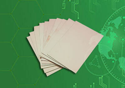
TPH-1/2는 특별한 공정과 복합을 통해 새로운 형태의 무기 및 유기 재료로 만들어집니다.
여기서 TPH-1/2를 사용하는 마이크로파 회로를 위한 설계의 장점:
(1) 기판은 검은색이다. 유전 상수는 2.65 이며, 광범위한 온도 및 주파수 범위에서 일관된 성능을 발휘합니다. 작동 온도는-100℃~+150℃입니다;
(2) 세라믹 기판의 진공 필름 코팅보다 동박와 기판 사이의 peel 강도가 더 신뢰할 수 있습니다. 이 기판은 고객에게 회로 처리가 용이하고, 생산 패스율이 높으며, 제조 비용이 세라믹 기판보다 훨씬 저렴하기 위해 만들어졌습니다.
(3) 소산 요인 tg δ ≤ 1 × 대 3, 그리고 손실은 약간의 빈도의 증가와 변동 일 뿐이다.
(4) 드릴, 펀치, 그라인드, 컷, 에칭 등을 포함한 기계 제조에 용이합니다.. 이러한 경우 세라믹 기판은 비교할 수 없습니다.
(5) 때문에 특정 중력 덜, 모듈의 주목할 만한 특성은이 기판에 의해 무게 더 가벼운 제조, 그러나 다른 재료는 비교할 수 없습니다.
(6) 동박 두께는:0.035 μ m
기술 사양:
Appearance | Smooth and neat on both sides: no stain,scratch and dent. | |||||
Dimension and tolerance (mm) | Dimensions and Tolerance | |||||
160×160±2mm 200×200±2mm | ||||||
Thickness and Tolerance | ||||||
δ(mm):2.5±0.075,3.0±0.1,4.0±0.1,5.0±0.2,6.0±0.12,7.0±0.15,8.0±0.15,9.0±0.2,10.0±0.2,12.0±0.2 | ||||||
For special dimensions,customized lamination is available. | ||||||
Mechanical Strength | Peel strength | In normal state:≥6N/cm;In the environment of alternating humidity and temperature:≥4 N/cm . | ||||
Chemical Property | According to the properties of laminate,the chemical etching method for PCB can be used. The dielectric properties of materials are not changed. | |||||
Electrical property | Name | Test condition | Unit | Value | ||
Density | Normal state | g/cm3 | 1.05 | |||
Moisture Absorption | Dip in distilled water of 20±2℃ for 24 hours | % | ≤0.02 | |||
Operating Temperature | High-low temperature chamber | ℃ | -100~+150(Processing temperature should not exceed 200℃) | |||
Thermal Conductivity | -55~288℃ | W /m /k | 0.3 | |||
CTE | 0~100℃ | ppm/℃ | 50(x,y,z) | |||
Shrinkage Factor | 2 hours in boiling water | % | 0.0004 | |||
Surface Resistivity | M.Ω | ≥1×10⁶ | ||||
Volume Resistivity | Normal state | MΩ.cm | ≥1×10⁹ | |||
Constant humidity and temperature | ≥1×10⁶ | |||||
Pin Resistance | 500V DC | Normal state | MΩ | ≥1×10⁶ | ||
Constant humidity and temperature | ≥1×101 | |||||
Dielectric Breakdown | kv | ≥20 | ||||
Dielectric Constant | 10GHZ | εr | 2.65(±2%) | |||
Dissipation Factor | 10GHZ | tgδ | ≤1×10⁻³ | |||
printed circuit board(PCB) with radio frequency(RF PCB) are an increasingly used technique within the PCB industry.
--RF pcb with a high frequency with works above 100 MHz.
--Microwave Circuit with works above 2 GHz radio frequency.
RF-pcb’s are used in different applications such as remote controls(wireless controls)security,smartphones,sensors etc.
New technologies make more and more use of these RF applications.
This asks for a manufacturing according to high quality standards and choosing the right RF materials depending on the application.
It is important that one knows the properties of the various materials.Choosing the right material is perhaps the most critical decision in the production process of the RF PCB.
ipcb advantage
1. Quick respond,24 hours online service
2. No MOQ requirement
3. Diverse capabilities
4. Fast turnarounds available
If you need microwave radio frequency PCB, click here Microwave Circuit.
