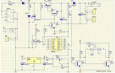
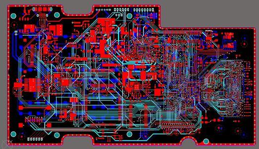
인쇄 회로 기판으로도 알려진 PCB는 전자 부품 간의 회로 연결 및 기능 구현을 실현할 수 있으며 전력 회로 설계의 중요한 부분이기도 합니다. ipcb는 이 백서에서 PCB 레이아웃 및 라우팅의 기본 규칙을 소개합니다.

1、 Basic rules of component layout
1. According to the layout of circuit modules, the related circuits that realize the same function are called a module. The components in the circuit module should adopt the principle of nearby concentration, and the digital circuit and analog circuit should be separated;
2. Elements and devices shall not be pasted within 1.27mm around the non installation holes such as positioning holes and standard holes, and components shall not be attached within 3.5mm (for M2.5) and 4mm (for M3) around the installation holes such as screws;
3. Do not arrange vias under the horizontal mounted resistors, inductors (plug-ins), electrolytic capacitors and other components, so as to avoid short circuit between the via holes and the component shell after wave soldering;
4. The distance between the outside of components and the edge of the board is 5mm;
5. The distance between the outside of the pad of the mounting element and the outside of the adjacent plug-in element is greater than 2mm;
6. Metal shell components and metal parts (shielding box, etc.) shall not collide with other components, and shall not be close to printed wire and pad, and the distance between them shall be greater than 2mm. The dimension of locating hole, fastener mounting hole, elliptical hole and other square holes in the plate to the plate edge is greater than 3mm;
7. The heating element should not be close to the wire and the heat sensitive element; the high-temperature device should be evenly distributed;
8. The power socket shall be arranged around the printed circuit board as far as possible, and the terminal of the power socket and the bus bar connected to it shall be arranged on the same side. Special attention should be paid not to arrange the power socket and other welding connectors between the connectors, so as to facilitate the welding of these sockets and connectors, as well as the design and wiring of power cables. The layout spacing of power socket and welding connector should consider the convenience of plug insertion and extraction;
9. Layout of other components:
All IC components shall be aligned on one side, and the polarity indication of polar components shall be clear. The polarity indication on the same printed circuit board shall not be more than two directions. When two directions appear, the two directions shall be perpendicular to each other;
10. When the density difference is too large, it should be filled with mesh copper foil, and the mesh should be more than 8mil (or 0.2mm);
11. There should be no through-hole on the pad to avoid solder paste loss and false soldering. Important signal lines are not allowed to pass through the socket pins;
12. The chip is aligned on one side with the same character direction and package direction;
13. Devices with polarity shall be marked with the same polarity direction on the same board as far as possible.

2、 Component routing rules
1. No wiring is allowed when the wiring area is less than or equal to 1 mm from the PCB edge and within 1 mm around the mounting hole;
2. The power line should be as wide as possible, and should not be less than 18mil; the signal line width should not be less than 12mil; the CPU in and out line should not be less than 10mil (or 8mil); the line spacing should not be less than 10mil;
3. The normal via hole was no less than 30mil;
4. Dual in-line: pad 60mil, aperture 40mil;
1 / 4W resistance: 51 * 55mil (0805 surface mount); 62mil pad and 42mil aperture when directly inserted;
Electrodeless capacitance: 51 * 55mil (0805 surface mount), 50mil pad and 28mil aperture when directly inserted;
5. Pay attention to the power line and ground wire should be radial as far as possible, and the signal line should not be looped.